Learn How to Make Your Own Electronics from Scratch starting with the Circuit Board Design
Curiosity is a sign of Genius, Glad you Made it!
Now further your mind into your skills and develop like a seed into a mighty force to be reckoned with!
Electronics run the world and our future, learn them!
Create Your Best PCB Design Altium
Transforming the Electronics Industry with Innovative PCB Design Software
From automotive and aerospace to consumer electronics and medical devices, Altium is always there for designers whenever and wherever.
iRobot (smart vac company) Overcomes PLM Integration Challenges with Altium
“This is what we’ve always been waiting for. The library parts are right here. I don’t have to go anywhere. I don’t have to sync. I can create my own projects. I can set up permissions for projects. We can work in smaller teams. We can do design reviews ourselves. All built into the tool.”
Create Your Best PCB Design at JLCPCB
Most Efficient, Economic, Innovative PCB Solutions
Founded in 2006, JLCPCB has been at the forefront of the PCB industry. With over 15-year continuous innovation and improvement based on customers’ need, we have been growing fast, and becoming a leading global PCB manufacturer, who provides the rapid production of high-reliability and cost-effective PCBs and creates the best customer experience in the industry at JLCPCB
Create Your Best PCB Design at LSCSC
LCSC was founded in 2011 in Shenzhen, China’s very own Silicon Valley, just bordering Hong Kong, China. It starts its business from a very small company. In the past 8 years since its founding, LCSC has grown into one of the largest electronic components distributors in China. Currently, LCSC has over 900,000 customers and over 310 employees with around $150 Million in sales. LCSC distributes over 200,000 products ranging from semiconductors to resistors, capacitors, diodes, inductors, connectors, transistors, sensors, providing design-chain services with EasyEDA too. EasyEDA is an easier and powerful online PCB design tool integrated LCSC component. LCSC acquired EasyEDA in March 2017. LCSC has been confirmed by ISO 9001: 2015. A new warehouse of 60,000 SQM equipped with smooth pick-and-ship operation system is expected in 2019.
RayPCB – manufacturing of Printed Circuit Boards, procurement of components
RayMing is China PCB assembly manufacturer,who offers complete PCB assembly services in Shenzhen, RayPCB’s capable of providing turn-key and partial turn-key printed circuit board assembly services.
For full turn-key, we take care of the entire process, including manufacturing of Printed Circuit Boards, procurement of components (100% original), PCBA Testing, continuous monitoring of quality and final assembly.
Whereas for partial turn-key, the customer can provide the PCBs and certain components, and the remaining parts will be handled by us.
EasyEDA – An Easier and Powerful Online PCB Design Tool
More than 5 million and continue creating components, letting you focus on the design, and you can create or import your own common libraries. Integrated LCSC and JLCPCB Component catalog Benefit from China’s leading electronic components distributor – LCSC ,and China’s leading PCB and SMT manufacturer – JLCPCB EasyEDA supports direct links to more than 800,000 real-time price, real-time inventory quantity components, During the design, the designers can refer to parts stocks, prices, values, datasheets and SMT information to shorten parts selection and project design cycles.
SparkFun Parts and Knowledge
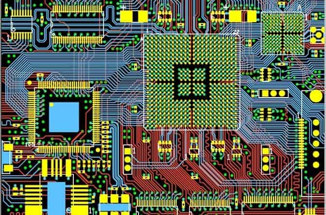
One of the key concepts in electronics is the printed circuit board or PCB. It’s so fundamental that people often forget to explain what a PCB is. This tutorial will breakdown what makes up a PCB and some of the common terms used in the PCB world. Learn more from Sparkfun or buy parts from Sparkfun
The electronic part search engine Octopart
Speed Up Your Product Design – housings and other stuff for your electronic design Onshape
Adafruit – Buy Weird stuff for your projects
Stop breadboarding and soldering – start making immediately! Adafruit’s Circuit Playground is jam-packed with LEDs, sensors, buttons, alligator clip pads and more. Build projects with Circuit Playground in a few minutes with the drag-and-drop MakeCode programming site, learn computer science using the CS Discoveries class on code.org, jump into CircuitPython to learn Python and hardware together, TinyGO, or even use the Arduino IDE. Circuit Playground Express is the newest and best Circuit Playground board, with support for CircuitPython, MakeCode, and Arduino. It has a powerful processor, 10 NeoPixels, mini speaker, InfraRed receive and transmit, two buttons, a switch, 14 alligator clip pads, and lots of sensors: capacitive touch, IR proximity, temperature, light, motion and sound. A whole wide world of electronics and coding is waiting for you, and it fits in the palm of your hand.
Have an amazing project to share? The Electronics Show and Tell is every Wednesday at 7pm ET! To join, head over to YouTube and check out the show’s live chat – we’ll post the link there.
Join us every Wednesday night at 8pm ET for Ask an Engineer!
Join over 36,000+ makers on Adafruit’s Discord channels and be part of the community! http://adafru.it/discord
Autodesk Fusion 360 PCB – One you get acquainted and feel like a pro go pro – PCB DESIGN SOFTWARE
Make anything with Autodesk Fusion 360 PCB design software. Powerful and accessible tools made for everyday engineering.
Printed circuit board (PCB) design brings your electronic circuits to life in the physical form. Using layout software, the PCB design process combines component placement and routing to define electrical connectivity on a manufactured circuit board. Autodesk Fusion 360 PCB
ChatGPT for Scripting – Coding for Newbies!
ChatGPT: Optimizing Language Models for Dialogue
We’ve trained a model called ChatGPT which interacts in a conversational way. The dialogue format makes it possible for ChatGPT to answer followup questions, admit its mistakes, challenge incorrect premises, and reject inappropriate requests. ChatGPT is a sibling model to InstructGPT, which is trained to follow an instruction in a prompt and provide a detailed response.
History of Circuitboards and Electronics

Today, building electronics systems that are simply functional is becoming an obsolete objective. Instead, the expectation that our devices and systems are “smart” is rapidly becoming the standard by which they are judged. These expectations are encapsulated in the concept of Ambient Intelligence (AmI), which can be thought of as the continual transformation of our environments into smart technological systems that are responsive to our needs and work cohesively to enhance our quality of life. The push towards this AmI destiny has affected the design and development of PCBs and electronic systems profoundly in recent history and is poised to be a driving factor for the foreseeable future.
With the deep entrenchment of electronics and printed circuit boards (PCBs) in our lives today, it would be understandable to assume that PCBs have been around for quite a while. This assumption, however, would be an error. In fact, the PCBs that we design and manufacture today have been with us for a scant few decades. Yet, we have been on the evolutionary road that has brought us here for over a century. Let’s take a look at the history of printed circuit boards to better understand this journey. You will probably be surprised by what we find!
Milestones in the History of Printed Circuit Boards
Below is a list of the inventors and companies whose ideas or developments have provided the most resounding impact in the history of printed circuits.
🗲 Albert Hanson invents first circuit board.
💡 Consisted of multiple layers.
💡 Utilized through-hole connectivity.
💡 Filed for a patent in 1903 in the United Kingdom.
🗲 Arthur Berry develops print and etch method in the United Kingdom.
💡 Patented in 1913.
🗲 Max Schoop, a Swedish inventor, develops a practical thermal spray
method.
💡 Developed a flame spray gun called the “pistol” in 1912.
💡 Patented a twin wire arc spray gun in 1914.
🗲 Charles Durcase creates means of electroplating circuits.
💡 Patented in 1927.
🗲 Paul Eisler invents the first contemporary printed circuit board.
💡 Developed a PCB for a radio system in 1936.
💡 United States uses technology during World War II for proximity fuses.
💡 U.S. Army releases printed circuit technology to the public in 1948.
🗲 Moe Abramson and Stanislaus F. Danko develop auto-assembly
process.
💡 Employed dip soldering process.
💡 Developed in 1949.
💡 Patent assigned to United States Army in 1956.
🗲 The Institute for Printed Circuits (IPC) is formed in 1957.
💡 The first organization to develop standards for PCB manufacture.
🗲 International Business Machines (IBM) introduces planar mounting.
💡 Developed in 1960.
💡 Originally developed for spacecraft.
💡 Becomes popular in the 1980’s as surface mount technology (SMT).
🗲 Gerber Scientific develops a PCB design format for vector
photoplotters.
💡 Gerber File format RS-274-D introduced in 1980.
💡 First widely accepted or standard PCB design file format.
💡 Two subsequent releases, X1 and X2, developed for CAM processing.
🗲 Vapor Computerized Systems introduces CAM software and file
format.
💡 Genesis 2000 software released in 1992.
💡 ODB++ data file format released to the public in 1997.
🗲 Multek introduces Every Layer Interconnect (ELIC) for high density
PCBs.
💡 Developed in 2006.
The above milestones in the history of printed circuits design and manufacturing have undoubtedly played significant roles in bringing the industry to the present. As with most historical examinations, there are some facts that seem to be elusive. For example, the question “Why are PCBs green?” is often asked. Although there is no clear consensus on a specific answer, there are solder mask considerations that support the green color. source
13 Basic Rules Of PCB Layout

1. According to the circuit module layout, the relevant circuit for realizing the same function is called one module, and the components in the circuit module should adopt the principle of near concentration, the digital circuit and the analog circuit are separated at the same time.
2. Do not mount the electronic components within 1.27mm around the non-mounting holes,such as tooling hole and standard holes.
Do not mount components within 3.5mm (for M2.5) and 4mm (for M3) around the mounting holes such as screws;
3.Avoid placing holes under the components such as the horizontally mounted resistors, inductors (insers), electrolytic capacitors, etc., so as to avoid short-circuiting the vias and component housings after wave soldering;
4.The distance between the outer side of the component and the edge of the pcb board is 5mm;
5. The outer side of the mounting component pad and the outer side of the adjacent interposing component are greater than 2 mm
6.Metal shell components and metal parts (shield boxes, etc.) can not touch other components, can not be close to the printed lines, pads, the spacing should be greater than 2mm. Positioning holes, fastener mounting holes, oval holes And the other side of the square hole outside the plate is larger than 3mm.
7.Heating componentscannot be in close proximity to the wire and the heating-sensitive components; the high-heating components should be evenly distributed;
8.The power socket should be placed around the printed circuit board as much as possible. The power socket and the bus bar terminal connected to it should be placed on the same side. Special care should be taken not to place the power socket and other solder connectors between the connectors to facilitate the connection. These sockets, connector soldering and power cable design and cable tie. The spacing between the power socket and the solder connector should be considered to facilitate the plugging and unplugging of the power plug (RayMing www.raypcb.com )

9. Other components:
All IC components are unilaterally aligned, and the polarity of the polar components is clearly marked. The polarity on the same printed board shall not be more than two directions. When two directions are present, the two directions are perpendicular to each other
10. the board surface wiring should be properly dense, when the difference between the density is too large, it should be filled with mesh copper foil, the grid is larger than 8mil (or 0.2mm);
11. There should be no through holes on the chip pads,avoid the solder joints from being lost due to solder paste loss. Important signal lines are not allowed to pass through the socket pins
12. the patch is unilaterally aligned, the characters are in the same direction, and the package direction is consistent
13. Polarized componentsshould be as consistent as possible in the direction marked by the polarity on the same board.
II.Rules of components wiring
1. Draw wiring in the area where the wiring area is ≤1 mm from the edge of the PCB board and within 1 mm around the mounting hole.
2. The power cord should be as wide as possible, should not be lower than 18 mil; signal line width should not be lower than 12mil; cpu input and output should not be lower than 10mil (or 8mil); line spacing is not less than 10mil;
3. The normal through hole should not less than 30mil;
4. Double in-line: Pad in 60mil, Aperture in 40mil;
1/4W resistor: 51*55mil (0805 surface mount);60mil when in-line of the PAD, aperture is 42mil;
Infinite capacitance: 51*55mil (0805 surface mount); 50mil in line of the PAD, aperture is 28mil;
5. The power line and ground should be as radial as possible, and the signal line can not appear loopback.